Defect detection is an integral part of wafer (chip) fabrication process. It enables defect detection and classification along the process to increase the fab yield (amount of good chips out of total wafers processed). Every detected defect is handled as an indicator of some process malfunction. This means that the defect itself cannot be repaired on its wafer occurrence. The process engineers should correct the process itself to avoid such defects.
Typical wafer defects are (each defect is categorized by its cause):
1. Too wide EBR (Edge Bead Removal)
2. Exposure Non-Uniformity
3. Solvent drips
4. Residues
5. Striations
6. Hot spots
7. Scribe or Array placement
8. Resist bubbles
9. Field tilt
10. Comets (scratches)
11. Particles
12. Off center resist dispense
13. (Macro) Peeling
14. (Macro) Scratch
15. (Macro) Large Particle
Once the defect is detected, it needs to be classified in order to enable the correction of the fabrication process. Classification is based on the defect properties such as specific patterns, geometries and similar. Some defects are part of a larger scenario as wafer scratch. In this case, a group of small, local defects form a larger event (defect). Pre-classification grouping is essential to ensure an accurate defect reporting. Defects that appear, on the wafer, as a set of small local defects, are designated Macro defects. As defined here, they are larger in size (magnitudes of difference) compared to the local, single-occurrence based, defects.
Wafer defect scanners are available today, built by high-end manufactures. Such scanners are highly accurate multi-discipline machines (electro-optical-computerized). They use various microscopy and lighting techniques to detect wafer defects in today’s most challenging technologies (as small as 10nM). The detection is based on pixel comparison on adjacent dyes or cells. Such high-resolution scanners are very expensive and (due to the high resolution used) the process of scanning the whole wafer is excessively slow. This leads to sampling-based defect detection operation: simply put, not every wafer is checked.
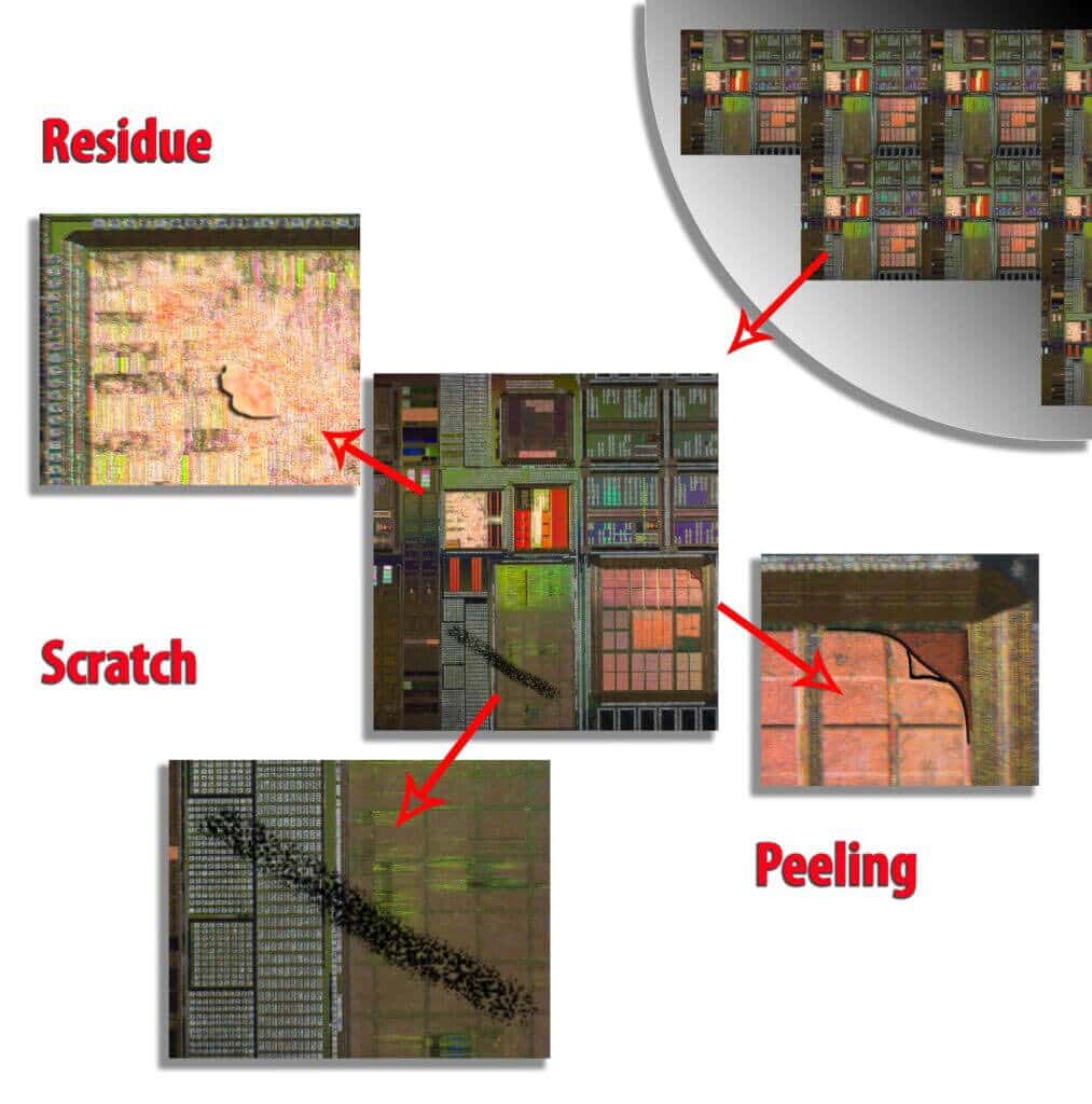
In recent years, additional type of defect detection scanners emerged. They are the Macro defect scanners. They are designed to handle the large scale (Macro) defects. Usually, the scanner is able to scan the wafer in a single FOV (Field of View). They are relatively cheaper, less complex (relative to the high-end defect scanners), easy to operate and have a faster operation cycle (i.e. full wafer scanning takes much less time). They can detect large defects but not a local small ones.
Macro defect scanning has its own function and advantages. Due to the fast scanning, every wafer can be checked. Usually, the operation is simpler and it does not require a complex recipe. Since the basic structure is composed of only a microscope, a camera and some handling mechanism, many companies entered this market and many products are available.
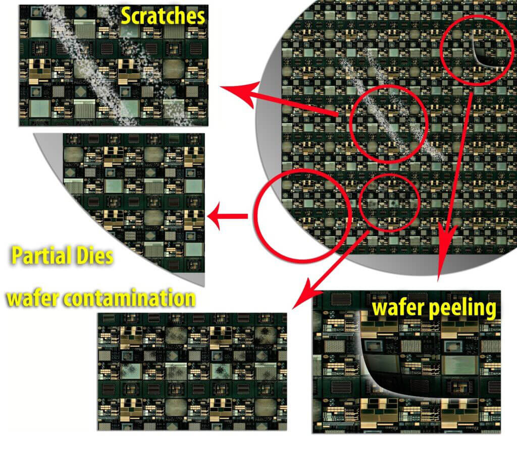
Automatic defect detection and classification is also required for Macro wafer defects. In this case, classical detection methods can be used (refer to pixel comparison above). However, deep learning technology used for defect classification may also be used for the detection process itself. This is due to the fact that, as opposed to high resolution scanning, we have the full FOV: the deep learning classifier can be trained to detect the Macro defects, based on their image signature. The whole operation, with deep learning, is faster and more accurate.
The CNN classifier is trained with a large set of samples for each defect type. They should contain many instances of the Macro defect over local wafer elements. For example, a wafer scratch (a type of Macro wafer defect) is passing over the wafer elements like metal tracks, silicon spacers and others. It is important to include samples for all the intermediate steps of the wafer fabrication. Also, re-training is essential to ensure the classifier will be up and running with new designs from new customers. Deep learning-based defect classification provides classifications free of human errors.
A CNN is configured to handle low-resolution images in order to maintain reasonable performance: for example, images of 300×300 pixels. The CNN is composed of 4 convolutional layers with linear activation. Follows a FC (Fully Connected) layer with sigmoid activation. Additional FC layers may be added, as required. The last layer is a SoftMax that provides the classification.
RSIP Vision is expert in both deep learning technology and wafer inspection; we have successfully achieved many computer vision projects for VLSI (wafer) equipment manufacturers.

